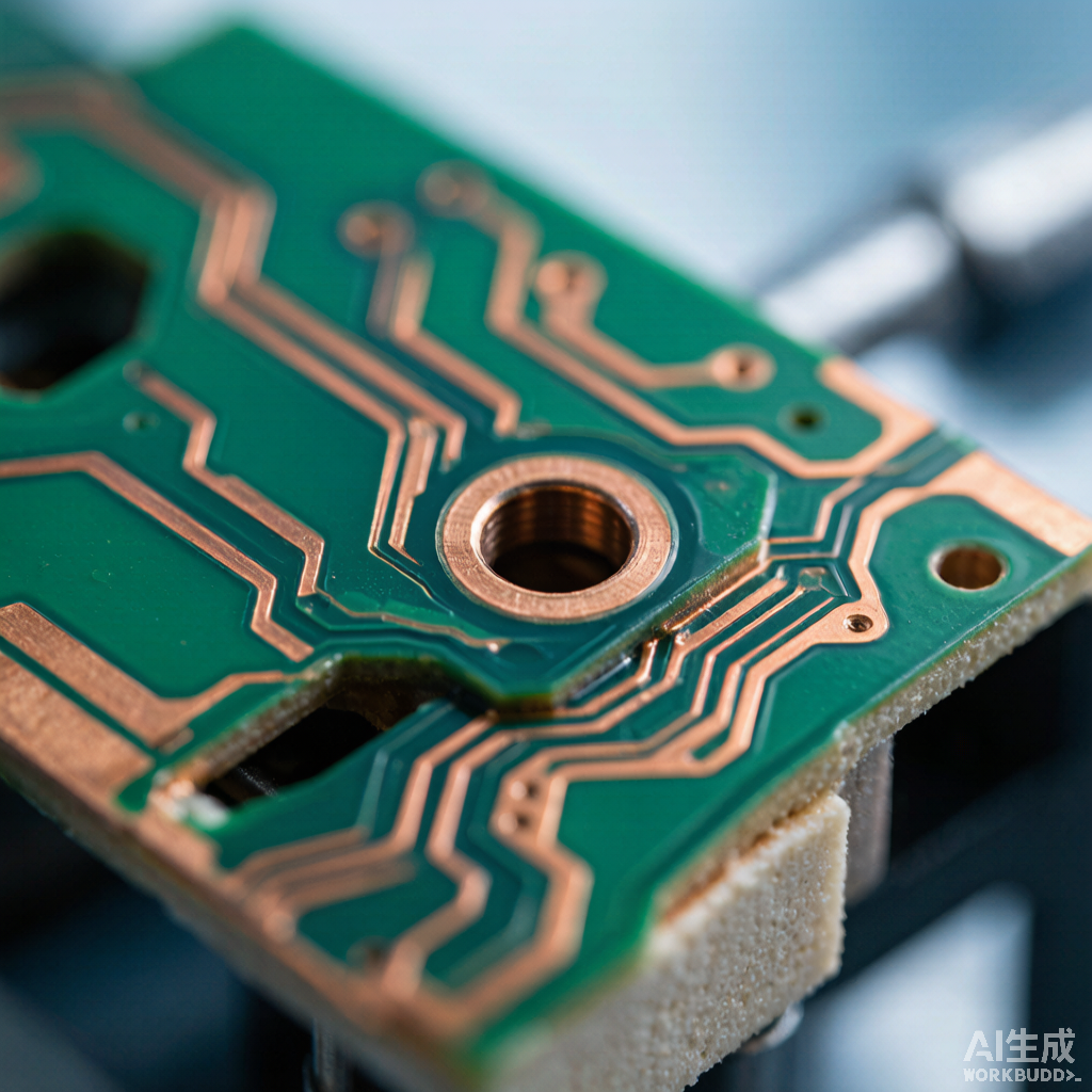
The Most Vulnerable Link in HDI Manufacturing: Why Microvias Deserve Your Full Attention
As electronic products continue to shrink in size while demanding higher performance, High-Density Interconnect (HDI) technology has become the backbone of modern PCB design. Traditional through-holes, which penetrate the entire board, consume valuable routing space on inner layers and lengthen signal paths. This is where microvia technology comes into play — enabling the dense, compact interconnects that today’s smart devices require.
At Gong Ming Electronic, we’ve spent 20 years manufacturing multilayer, HDI, and high-frequency PCBs. This article explains what microvias are, how they’re manufactured, and — most importantly — the five common defects that make them the most vulnerable link in the entire HDI production chain, along with practical engineering countermeasures.
1. What Is a Microvia?
A microvia is a small hole that connects only the outer layer to the adjacent inner layer, without penetrating through the entire board. In simpler terms, it starts at the board surface and terminates at a specific inner layer — you cannot see it from the opposite side. This distinguishes it from a buried via, which is completely hidden between inner layers and invisible from both sides of the board.
By industry convention, a via is classified as a microvia when its diameter is less than or equal to 0.15 mm (approximately 6 mils) and its depth does not exceed its diameter. Microvias are typically formed using laser drilling, which offers significant advantages over mechanical drilling: smaller and more precise holes, and a much smaller heat-affected zone around the drilled area.
Microvias are the defining feature of HDI boards. In a typical “one-step” HDI board, the connection between the outer layer and the second layer relies entirely on microvias. Higher-order HDI boards stack microvias across multiple layers, creating what are known as stacked via or staggered via structures.
2. The Microvia Manufacturing Process
A typical microvia manufacturing flow proceeds as follows: after inner-layer circuitry is completed and laminated, a laser ablates the copper foil and resin at the target locations, exposing the copper pad on the inner layer beneath. The hole is then subjected to desmear — removing residual molten resin at the hole bottom — followed by electroless copper deposition and electroplating to build up a copper layer on the hole wall, establishing electrical connection between the outer and inner layers.
This process may sound straightforward, but every single step carries hidden risks — as the five defect families below demonstrate.
3. Common Microvia Defects and Their Causes
3.1 Hole-Bottom Residue and Poor Connection
This is the most common — and most fatal — microvia defect. After laser drilling, the hole bottom often retains incompletely vaporized resin debris or re-solidified molten resin residues. If the desmear process is not thorough, these residues block subsequent copper deposition, resulting in an open circuit or high-resistance contact between the hole-bottom copper and the inner-layer pad.
Field experience: In actual failure analysis, a typical failure mode is “hole-bottom separation” — cross-sectioning reveals a fine crack between the hole-bottom copper and the inner-layer copper pad under the microscope. This defect may escape continuity testing before shipment (because a temporary contact still exists), but under SMT reflow or in-service thermal stress, the crack opens completely. This is precisely why HDI boards require additional thermal stress or thermal cycling reliability testing.
3.2 Poor Hole Shape and Rough Hole Walls
Excessive laser energy or incorrect focal distance results in irregular hole shapes, flared openings, or overly rough hole walls. Rough walls cause uneven plating during subsequent electroplating, with thinner copper at sharp corners — creating potential stress concentration points and open-circuit risks. Conversely, insufficient laser energy may leave holes incompletely drilled, failing to fully expose the inner-layer copper.
Field experience: Different laminate materials have vastly different laser absorption rates. Standard FR-4 is relatively easy to process, but high-Tg materials or boards with fillers require higher laser energy and tend to produce more residue. Engineers should prioritize laminate grades that are certified and optimized for laser drilling when designing HDI boards.
3.3 Misregistration
A microvia must be drilled precisely at the center of the inner-layer pad beneath it. If the laser drilling alignment system lacks precision, or if the material shrinks or deforms during lamination, the microvia may land outside the pad — hitting adjacent resin or even inner-layer traces. In this case, the connection area between the microvia and the inner-layer pad is reduced or lost entirely, along with a risk of short circuits.
Field experience: Always provide sufficient pad-size margin for microvias in your design. For a 0.1 mm microvia, the inner-layer pad diameter should generally be no less than 0.3 mm. This accommodates up to ±0.1 mm of misregistration without the via drifting off the pad. Many PCB prototyping failures trace back to pads designed too small for the fabricator’s alignment capability.
3.4 Stress Concentration and Cracking in Stacked Vias
In higher-order HDI boards, multiple microvias overlap across different layers. For example, in a three-step HDI board, the surface microvia sits directly above a second-layer microvia, which in turn sits above a third-layer microvia. Stacked-via structures endure far greater mechanical and thermal stress than ordinary through-holes during lamination, reflow, and thermal cycling. The copper at stacked-via junctions repeatedly undergoes tensile and compressive cycling, eventually developing micro-cracks that propagate into open circuits.
Field experience: Unless absolutely necessary, prefer staggered via designs over stacked vias. Staggered vias offset the stress-bearing positions across layers, distributing stress more evenly. If stacked vias are unavoidable, add a solid copper pad beneath the stack as support, and use resin-filling plus re-plating (the “copper filled and plated over” process) between each stacked layer — though this significantly increases manufacturing cost.
3.5 Voids and Delamination
During microvia plating, if air inside the hole is not fully evacuated or moisture removal is incomplete, trapped air forms tiny bubbles in the plating bath that block copper deposition, causing recessed walls or copper-free areas. Additionally, thermal stress from laser drilling can cause localized separation at the resin-copper foil interface, which may develop into visible delamination during subsequent thermal processes.
Field experience: Microvia quality depends heavily on process experience. The same design can yield dramatically different microvia reliability across different factories. It is strongly recommended to run a DOE (Design of Experiments) validation before mass production, and to evaluate the process window through cross-sectioning (at least 5 microvias per panel) and thermal stress testing (288°C solder float for 10 seconds without wall cracking).
4. Conclusion: Design for Reliability
Microvias are the soul of HDI boards — and the most vulnerable link in the entire PCB manufacturing chain. Their processing challenges are numerous: extremely small diameters, aspect ratios approaching 1:1, stringent hole-bottom cleanliness requirements, demanding alignment precision, and difficult subsequent plating and filling.
For electronics engineers, understanding these microvia processing challenges enables smarter decisions at the design stage — allocating adequate pad margins, minimizing unnecessary stacked vias, selecting laser-drilling-compatible laminates, and communicating with your fabricator to confirm their microvia process capability. Only then can high-density design truly translate into high-reliability products.
Partner With a Manufacturer That Masters Microvia Manufacturing
At Gong Ming Electronic, we don’t just drill microvias — we control the entire process window behind them. With over 20 years of PCB manufacturing experience, ISO 9001 and IATF 16949 certifications, and a factory expanding to 3x capacity in 2026, we deliver HDI boards with the reliability your designs demand.
Our engineering team provides DFM feedback that goes beyond simple pass/fail — we help you optimize pad sizes, via stacking strategy, and laminate selection before production begins, so microvia defects never reach your assembly line. Whether you need one-step HDI for consumer electronics, stacked-via designs for high-density computing, or laser-drilling-optimized laminates for demanding applications, our process expertise ensures your design performs as intended.
Ready to discuss your HDI project? Get a quote within 24 hours — our engineering team will review your design and provide DFM feedback at no cost.